|
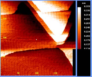
Left: A well-prepared Au(111) surface (200 X 200
nm2) shows large terraces and steps. The monatomic
step height of 2.5 E is shown. Domain boundaries between regions
with hcp and fcc type atomic stacking are seen as pairwise bright
stripes. The sample was prepared by repeated cycles of Ar+
sputtering at 1kV and annealing in vacuum at 1000K.
|
|
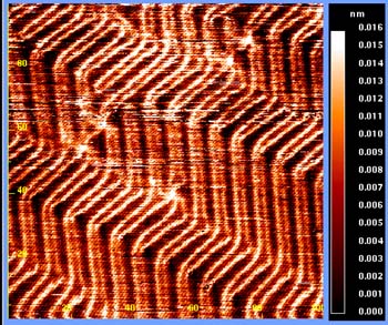
Left: This detailed image shows periodic rotational
domains(120 °), zigzag pattern (100 x 100 nm2).
|
|
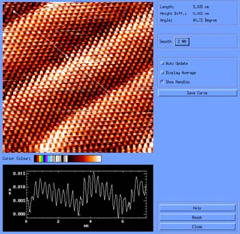
Left: Atomic resolution STM image of the 2343
reconstructed Au(111) surface (848 nm2). Atomic
corrugation 0.15 E; tunneling current 0.3 nA; scanning voltage 0.3
V.
|