Assembly of Nanostructured Materials and Devices
This effort focuses on the
directed and self assembly of nanomaterials from nanocomponents. This includes the patterned and unpatterned films and of device structures of
nanocrystals by using electrophoretic deposition and of carbon nanotubes and of nanowires by dielectrophoretic deposition. The Herman group is also interesting in the optical, electrical, and mechanical properties of these nanostructured materials and arrangements.
Also, see
publications, including #96, 100, 109, 113, 114, 116, 119, 124, 126, 128, and 130-138.
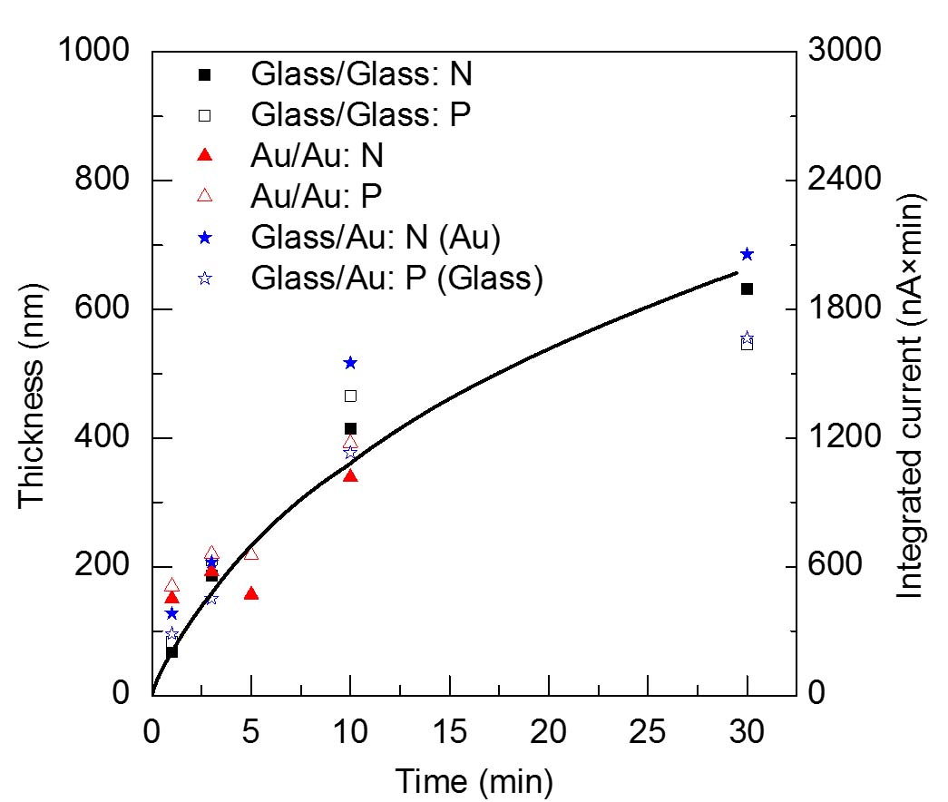
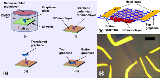
Fabricating Quantum Dot Monolayers Sandwiched Between van der Waals Monolayer Electrodes
Using methods to form order monolayers of quantum dots on a liquid surface,
the Herman group made sandwiches of a monolayer of CdSe quantum dots (or nanoparticles) between two graphene layers,
as shown in the below figure. This is a new type of vertical heterostructure made of nanocomponents, which can provide
new functionality.
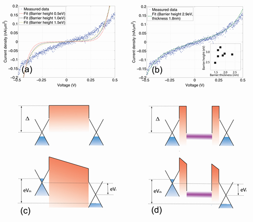
This heterostructure has an tunneling type of I-V behavior (as seen in the below figure).
For more, see
Electronic Transport in Nanoparticle Monolayers Sandwiched Between Graphene Electrodes,
C. Lu, D. Zhang, A. van der Zande, P. Kim and I. P. Herman,
Nanoscale 6, 14158-14162 (2014).
Back to top
|
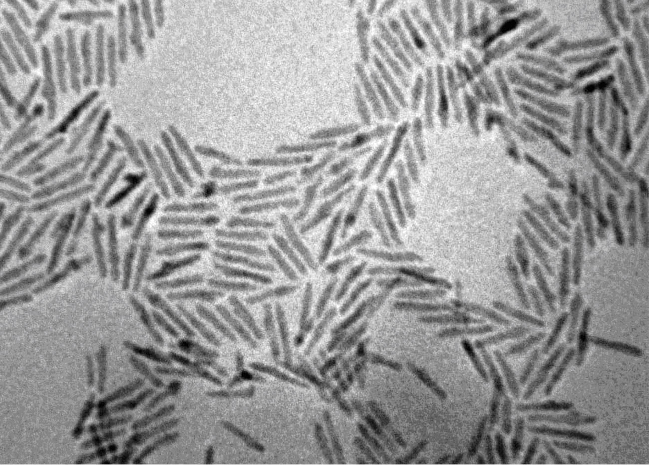
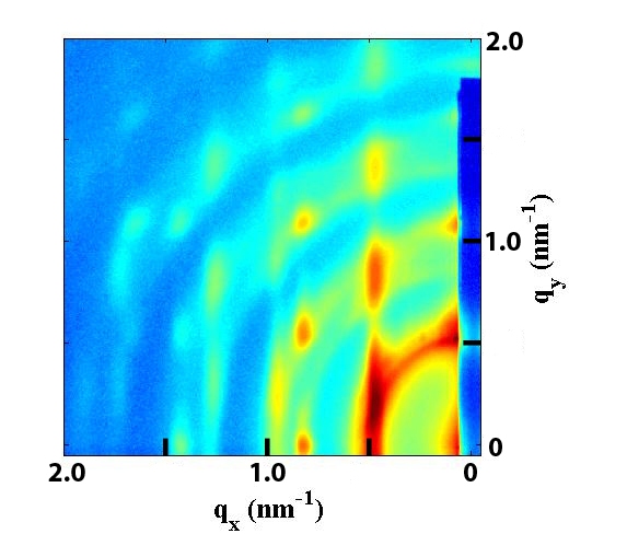
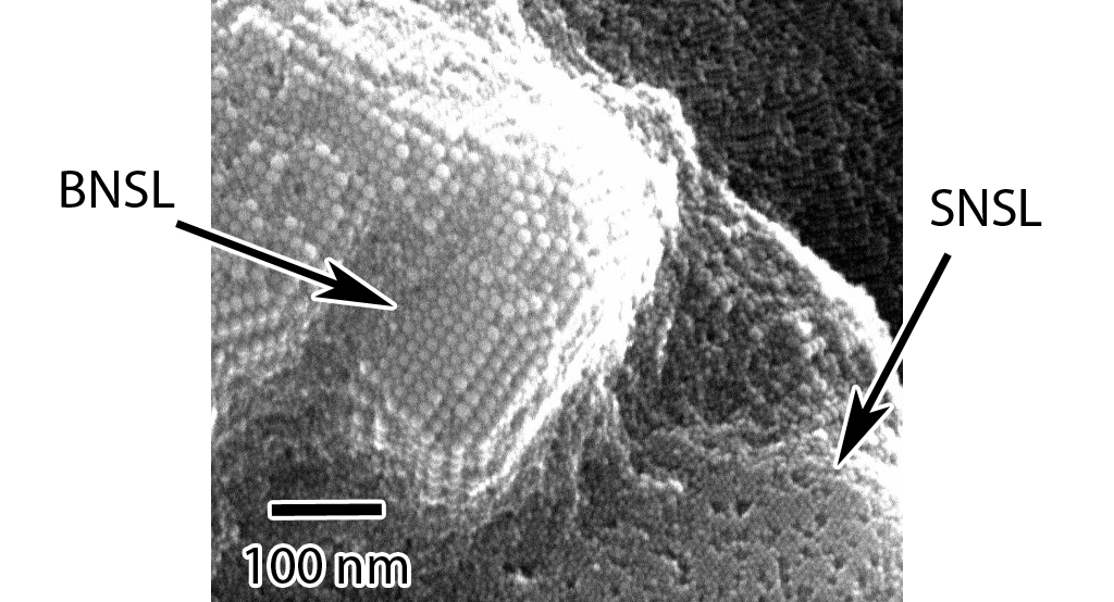
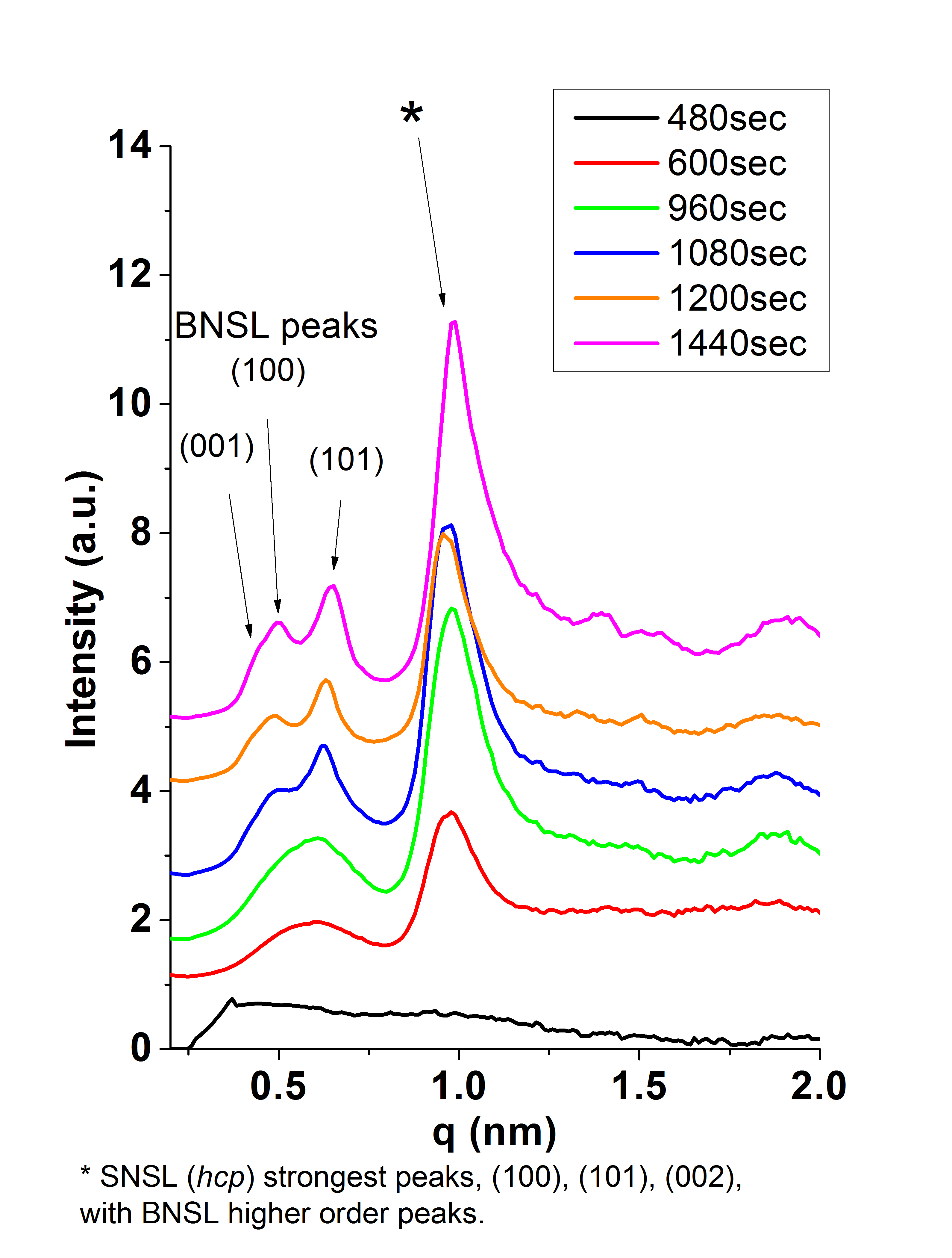
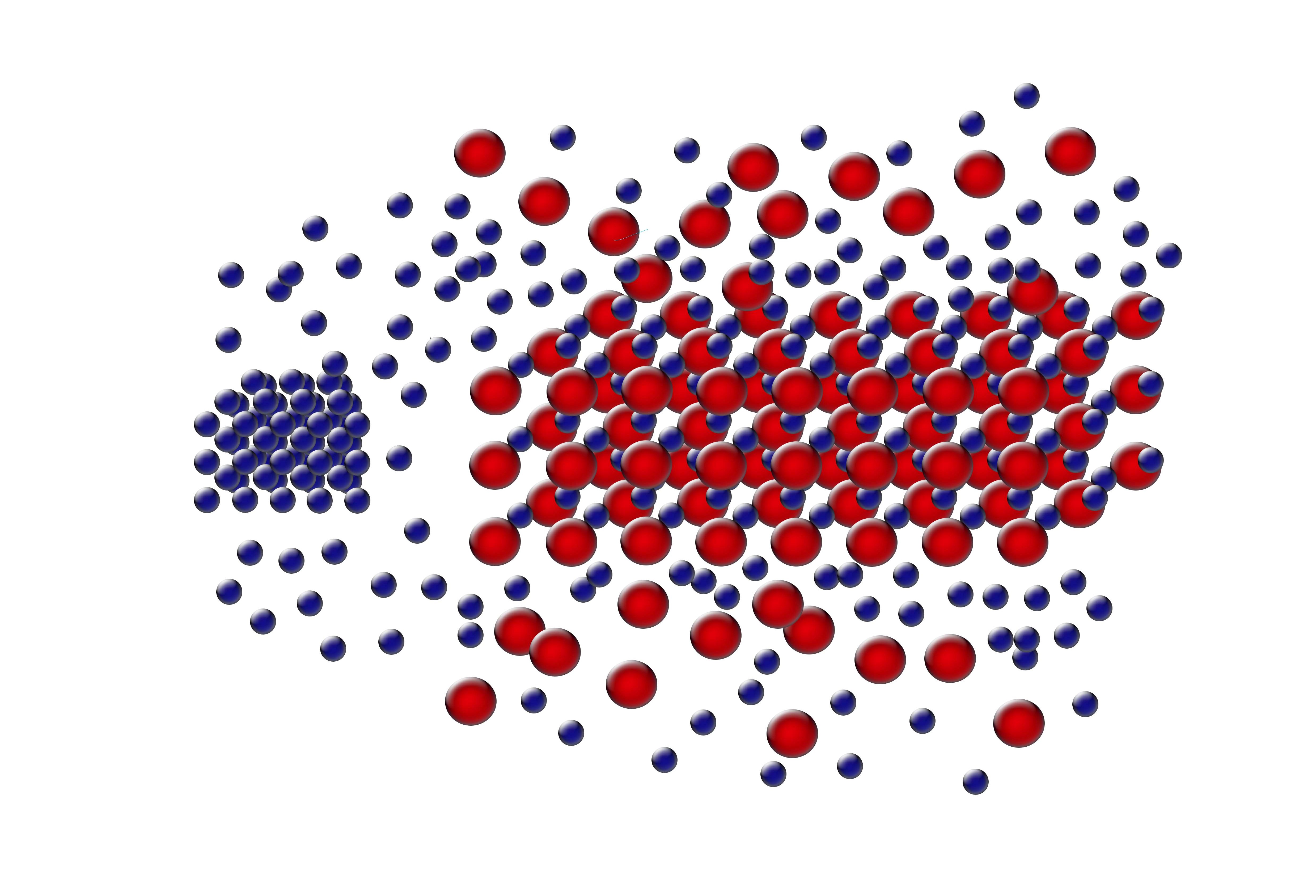
SAXS Monitoring Growth of Thick Single and Binary Nanoparticle Superlattices
Using small angle x-ray scattering (SAXS) at the
Brookhaven National Laboratory
the Herman group has followed in real time the kinetics of the growth of ordered
3D NP superlattices (SLs, SNSLs) (of one size of iron oxide NPs) and binary NP SLs (BNSLs)
(of two sizes of iron oxide NPs)
in solution are understood by combining controlled solvent evaporation.
We have learned that
the larger the NP the farther apart are the NPs when
the SNSLs begin to precipitate and the closer they are after ordering, as seen in the below figures,
which we have explained
by using a model of the energies of interactions betweent the NPs.
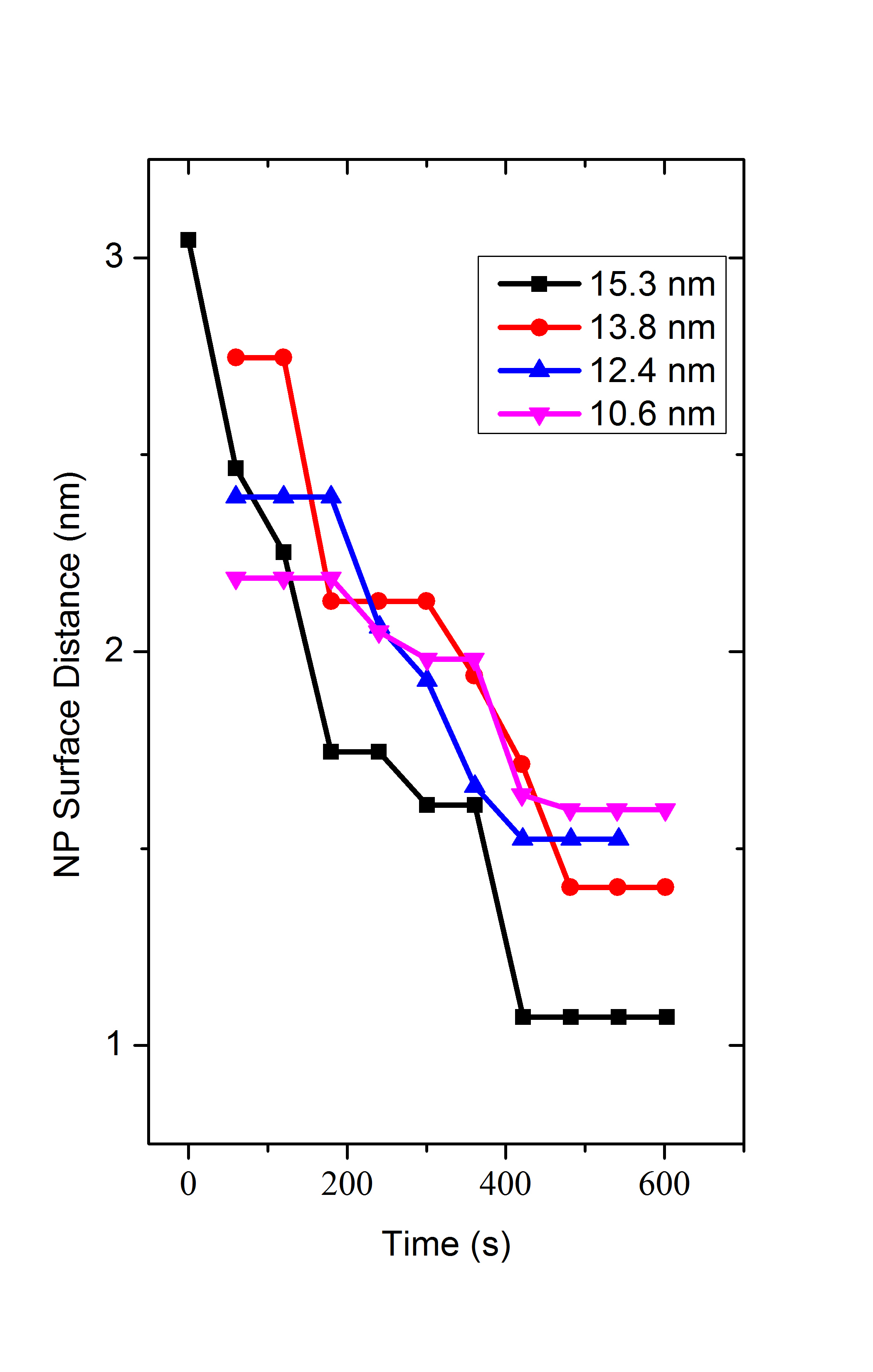
When forming BNSLs of two different sized NPs, the NPs that are in excess of that needed
to achieve the final BNSL stoichiometry are expelled during the BNSL formation
and these expelled NPs can form SNSLs (as seen in the below figures).
For more, see
Resolving the Growth of 3D Colloidal Nanoparticle Superlattices by Real-time Small Angle
X-ray Scattering,
C. Lu, A. J. Akey, C. Dahlman, D. Zhang, and I. P. Herman,
J. Am. Chem. Soc. 134, 1873218738 (2012).
Back to top
|
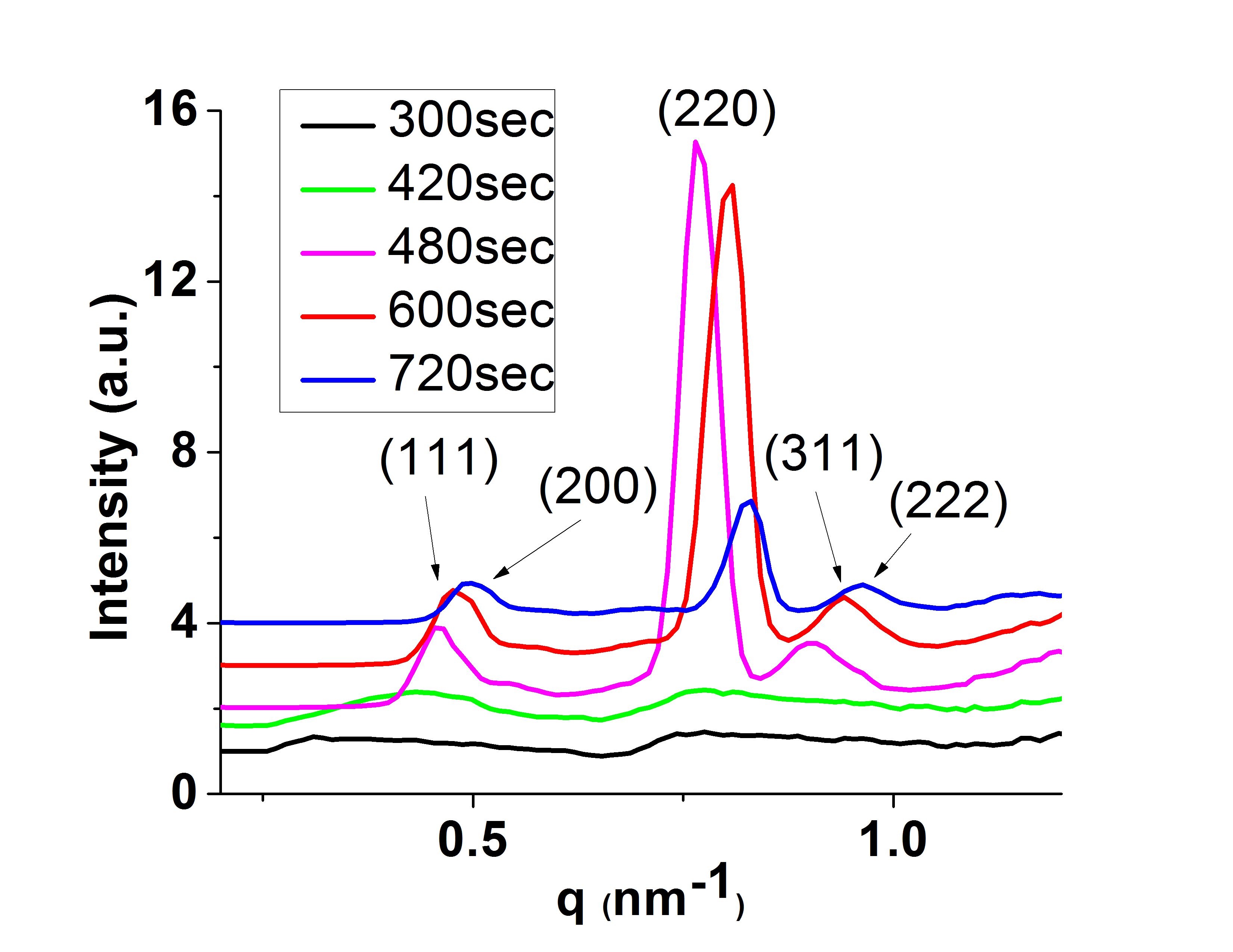
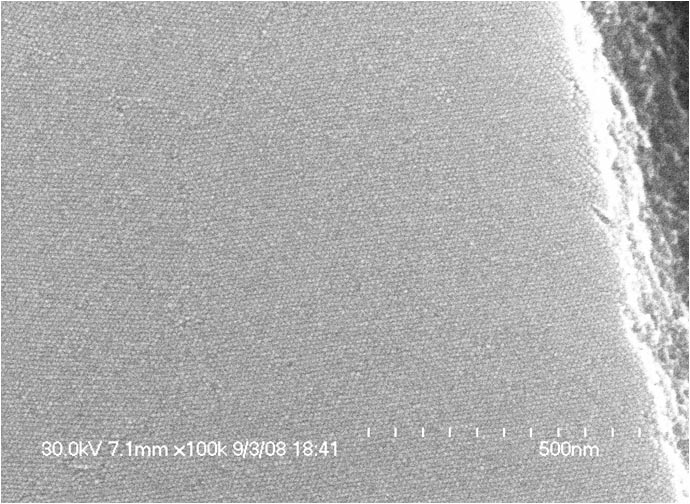
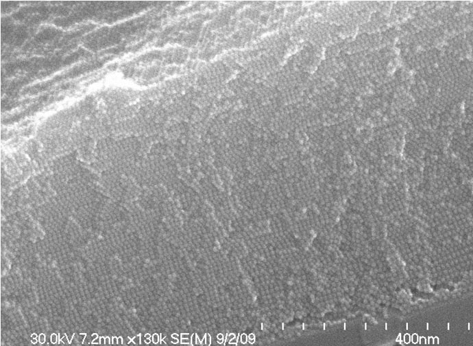
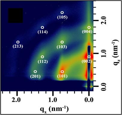
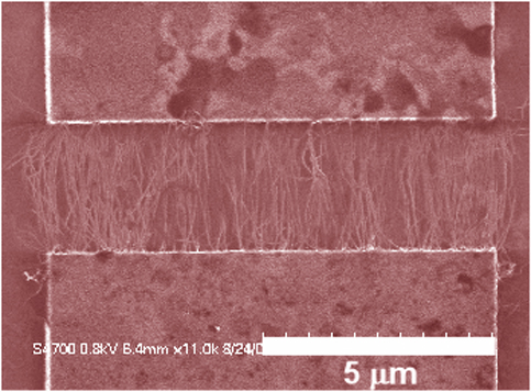
Precisely Placed 100-Layer Thick Nanocrystal Superlattices
The Herman group has developed a method to form 100-layer thick supercrystals of nanoparticles
at lithographically-determined sites using a two-solvent microfluid flow method. These micrometer-dimension supercrystals
form as a result of flow from a reservoir to a channel (due to capillary flow) and subsequent controlled drying.
Previously, very few layered-superlattices could be formed on surfaces and supercrystals could be formed only after drying in beakers.
These new materials open the prospect of cooperative optical, electrical, magnetic and magenetic properties.
The left SEM shows the top of a CdSe nanocrystal superlattice
and the right one shows the side of a cleaved Fe2O3 nanocrystal superlattice.
The trace represents small angle x-ray scattering (SAXS) of the Fe2O3 nanocrystal superlattice.
For more, see
Formation of Thick, Large-Area Nanoparticle Superlattices in Lithographically Defined Geometries, A. Akey, C. Lu, L. Yang, and I. P. Herman,
Nano Lett. 10, 1517 (2010).
Back to top
|
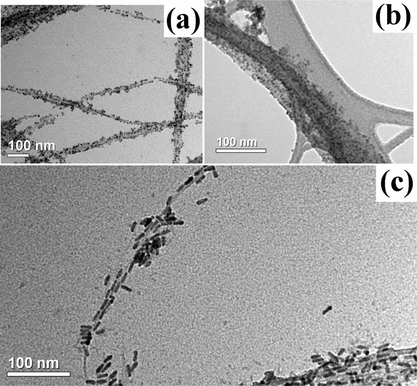
Formation of Nanocrystal-Carbon Nanotube Hybrid Materials
The Herman group is using methods to form hybrids of nanocrystals and carbon nanotubes that may have novel optical
and electrical properties. Both components have signature optical properties and coupling between them may be very interesting.
The left SEM shows HIPCo carbon nanotubes with (a) CdSe nanparticles, (b) core shell particles and (c) CdSe nanorods,
and the right SEM shows a hybrid of a CNT and CdSe nanoparticles on a surface, with an AFM inset.
For more, see
Versatile Formation of
CdSe Nanoparticle-Single Walled Carbon Nanotube Hybrid Structures, C. Lu, A. Akey, W. Wang, and I. P. Herman,
J. Am. Chem. Soc. (Commun.) 131, 3446 (2009).
Back to top
|
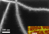
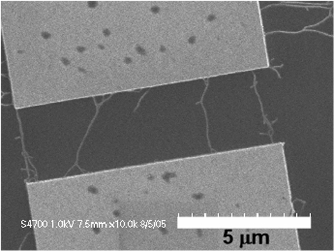
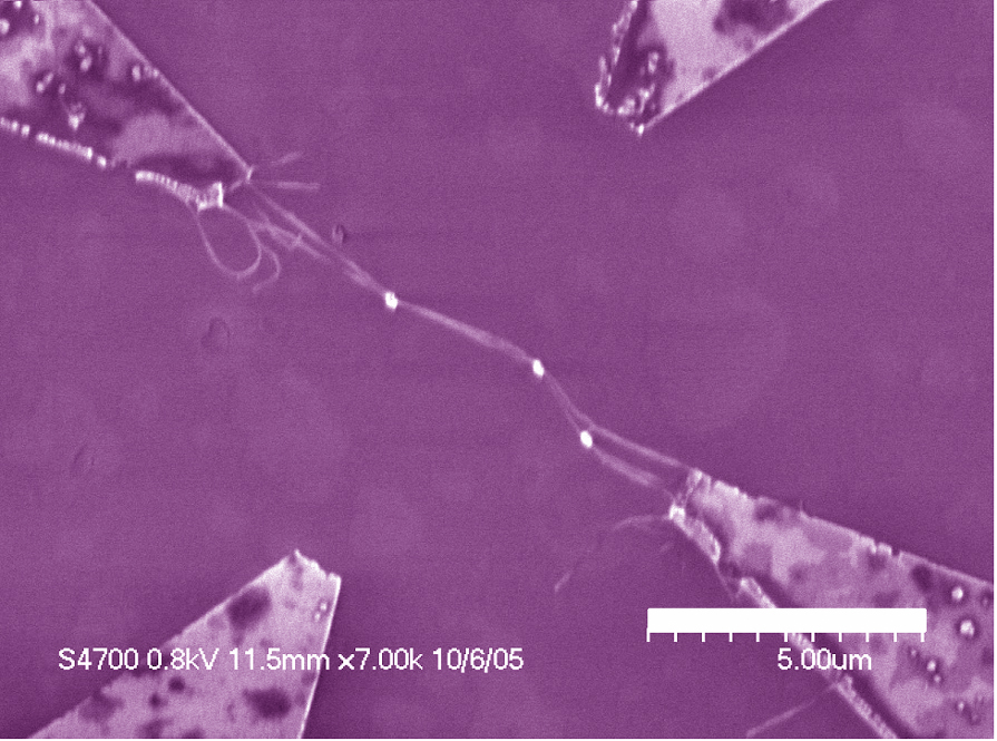
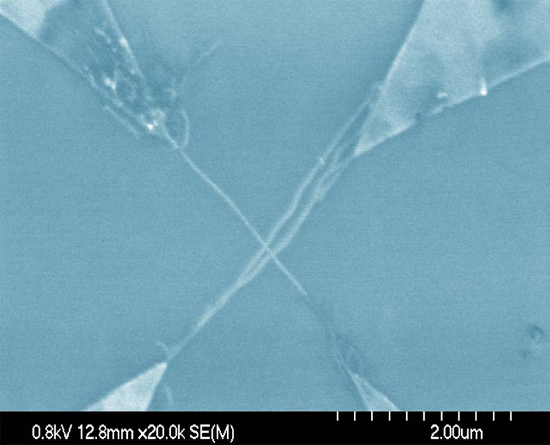
Spatially Controlled AC Dielectrophoretic Placement of Carbon Nanotubes in Device Structures
The Herman group is developing and using methods to controllably place single walled carbon nanotubes (CNTs) in multi-electrode device geometries by using dielectrophoretic deposition (DEPD) and other methods. The top row shows SEMs of DEPD without (left) and with (right) control by series resistors. The bottom row shows control using floating posts (left) and controlled deposition of crossed CNTs (right).
For more, see
"Precise Positioning of Carbon Nantoubes by AC Dielectrophoresis Using Floating Posts" S. Banerjee, B. White, L. Huang, B. J. Rego, S. OBrien, and I. P. Herman, Appl. Phys. A 86, 415-419 (2007) and Precise Positioning of Single-Walled Carbon Nantoubes by AC Dielectrophoresis, S. Banerjee, B. White, L. Huang, B. J. Rego, S. OBrien, and I. P. Herman, J. Vac. Sci. Technol. 24, 3173 (2006).
Back to top
|
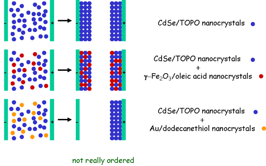
Electrophoretic Deposition of Films of Mixtures of CdSe and Fe2O3 Nanocrystals
In some cases,
electrophoretic deposition using mixtures of nanocrystals produces
films composed of mixtures of the nanocrystals. This is shown below
schematically for mixtures of CdSe and Fe2O3
nanocrystals. Such film mixtures are potentially multifunctional
nanomaterials. When Au nanocrystals are added to a hexane solvent
containing either CdSe or Fe2O3 nanocrystals, there is deposition of a film containing either only CdSe or Fe2O3 nanocrystals, respectively, and this occurs on only one electrode. This is a collaboration with the O'Brien and Levicky groups.
For more, see "Addition, Suppression, and Inhibition in the Electrophoretic
Deposition of Nanocrystal Mixture Films for CdSe Nanocrystals with γ-Fe2O3 and Au Nanocrystals,"
M. A. Islam, Y. Xia, M. L. Steigerwald, M. Yin, Z. Liu, S. O'Brien, R. Levicky, and I. P. Herman,
Nano Letters 3, 1603-1606 (2003).
Back to top
|
|
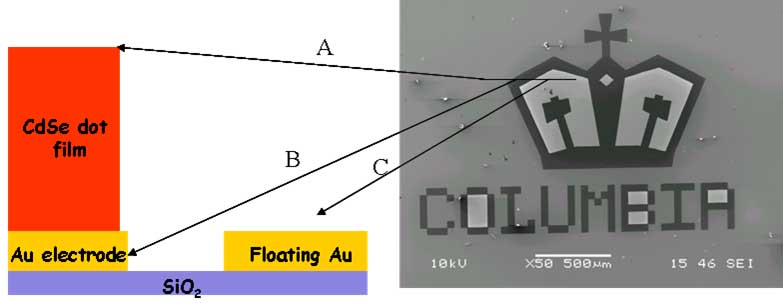
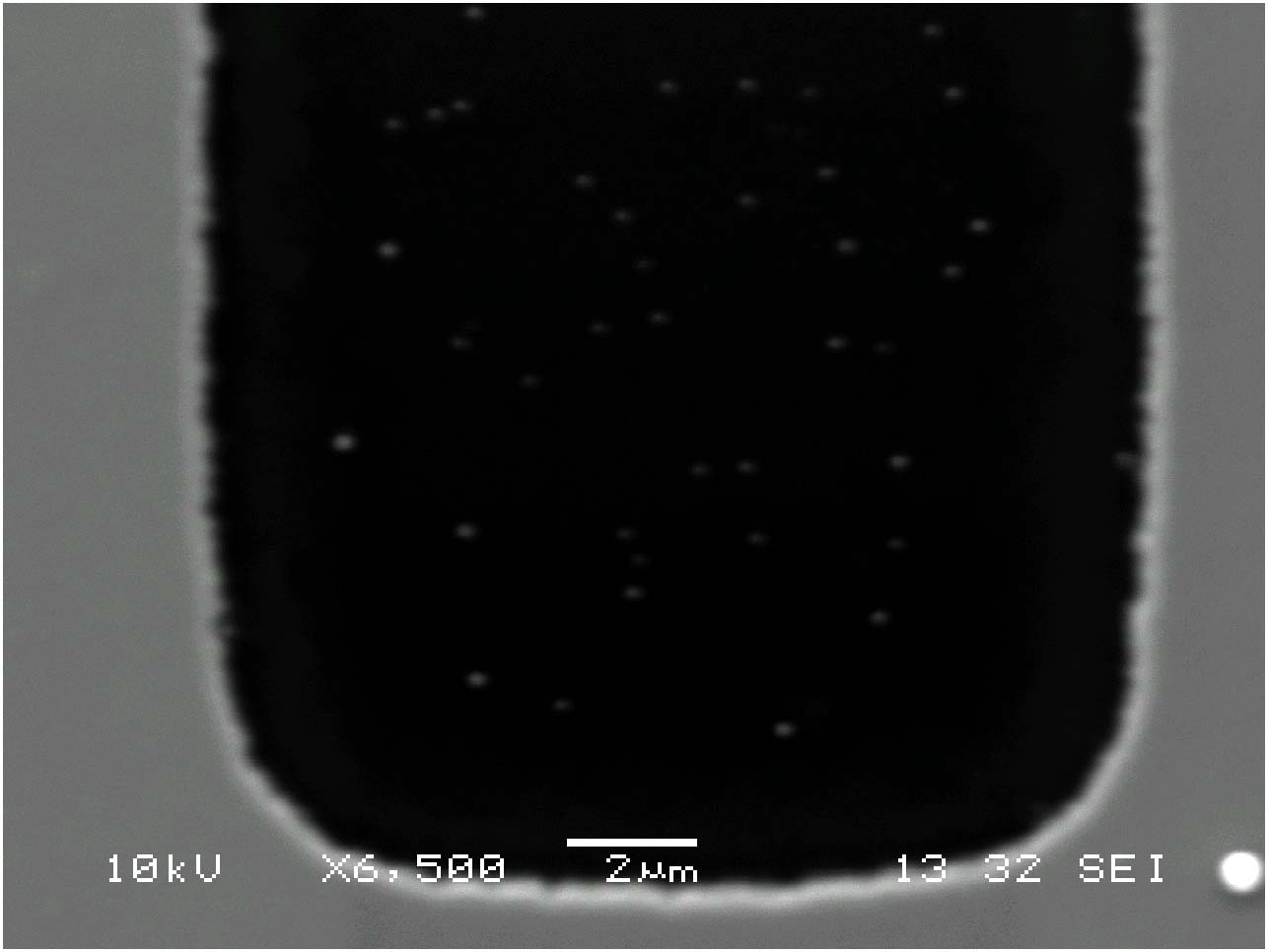
The Herman group is
examining the use of electrophoretic deposition methods to form thick,
smooth, robust films of CdSe nanocrystals. The figure on the top shows
particles selectively depostied on metal regions in contact with the
electrode (gray), with no deposition on oxide (dark) or metal regions
isolated from the electrode (bright). Depositon about of a particle
film (gray) around an oxide spacer (dark) is shown on the bottom. For
very thick films, strain leads to film fracture, as is seen in the SEM
(lower, right). Such cracking is not uncommon when there is some
solvent evaporation during film drying.
For more, see
"Electric-Field Assisted Deposition of Patterned Nanocrystal Films using Thermally Charged CdSe Nanocrystals,"
M. Islam and I. P. Herman, Appl. Phys. Lett. 80, 3823-3825 (2002) and "Controlled Electrophoretic Deposition of Smooth and Robust Films of CdSe Nanocrystals,"
M. A. Islam, Y. Xia, D. A. Telesca, Jr., M. L. Steigerwald, and I. P. Herman,
Chem. Mater 16, 49-54 (2004).
Back to top
|
Real-time Monitoring of Organic Surface Ligands and Solvent During the Self-Assembly of Nanocrystal Arrays
The densities of
surface ligands and solvent molecules are being followed during the
self-assembly of CdSe nanocrystals into arrays by using
multiple-reflection attenuated total internal reflection (ATIR)
spectroscopy. This is performed in a Fourier transform infrared (FTIR)
spectrometer in which the arrays formed on a ZnSe prism. During the
self-assembly of CdSe nanocrystals passivated by pyridine that are
dissolved in pyridine, the 1436.1 cm-1 peak of neat pyridine is followed along with that at 1445.2 cm-1 due to pyridine bound to the CdSe surface (below).

The
solvent evaporates in about 30 minutes during the self-assembly of
~200-monolayer thick arrays in an argon ambient (inset below). The
pyridine bound to the surface slowly leaves the surface (inset, open
symbols), but about 35% remains after drying for several days (main
figure, below). Since pyridine only weakly binds to the surface, it had
been commonly thought that no pyridine would remain after extensive
drying. While this is not true, there are still significant changes to
the surface during drying. This result is important for the MRSEC
studies of the self-assembly of arrays and the properties of these
arrays. This monitoring method is also being used to follow the surface
of exchange of TOPO and pyridine ligands, and related processes.

For more, see
"Organic Ligand and Solvent Kinetics during the Self Assembly
of CdSe Nanocrystal Arrays using Infrared Attenuated Total Reflection,"
B. Kim, L. Avila, L. Brus, and I. P. Herman, Appl. Phys. Lett. 76,
3715-3717 (2000).
Back to top
|